Transistor
Introduction
Transistors make our electronics world go ‘round. They’re critical as a control source in just about every modern circuit. Sometimes you see them, but more-often-than-not they’re hidden deep within the die of an integrated circuit. In this tutorial we’ll introduce you to the basics of the most common transistor around: the bi-polar junction transistor (BJT).
 In small, discrete quantities, transistors can be used to create simple electronic switches, digital logic, and signal amplifying circuits. In quantities of thousands, millions, and even billions, transistors are interconnected and embedded into tiny chips to create computer memories, microprocessors, and other complex ICs.
Transistors make our electronics world go ‘round. They’re critical as a control source in just about every modern circuit. Sometimes you see them, but more-often-than-not they’re hidden deep within the die of an integrated circuit. In this tutorial we’ll introduce you to the basics of the most common transistor around: the bi-polar junction transistor (BJT).
In small, discrete quantities, transistors can be used to create simple electronic switches, digital logic, and signal amplifying circuits. In quantities of thousands, millions, and even billions, transistors are interconnected and embedded into tiny chips to create computer memories, microprocessors, and other complex ICs.
Covered In This Tutorial
After reading through this tutorial, we want you to have a broad understanding of how transistors work. We won’t dig too deeply into semiconductor physics or equivalent models, but we’ll get deep enough into the subject that you’ll understand how a transistor can be used as either a switch or amplifier.
This tutorial is split into a series of sections, covering:
- Symbols, Pins, and Construction – Explaining the differences between the transistor’s three pins.
- Extending the Water Analogy – Going back to the water analogy to explain how a transistor acts like a valve.
- Operation Modes – An overview of the four possible operating modes of a transistor.
- Applications I: Switches – Application circuits showing how transistors are used as electronically controlled switches.
- Applications II: Amplifiers – More application circuits, this time showing how transistors are used to amplify voltage or current.
There are two types of basic transistor out there: bi-polar junction (BJT) and metal-oxide field-effect (MOSFET). In this tutorial we’ll focus on the BJT, because it’s slightly easier to understand. Digging even deeper into transistor types, there are actually two versions of the BJT: NPN and PNP. We’ll turn our focus even sharper by limiting our early discussion to the NPN. By narrowing our focus down – getting a solid understanding of the NPN – it’ll be easier to understand the PNP (or MOSFETS, even) by comparing how it differs from the NPN.
Suggested Reading
Before digging into this tutorial, we’d highly recommend giving these tutorials a look-through:
- Voltage, Current, Resistance, and Ohm’s Law – An introduction to the fundamentals of electronics.
- Electricity Basics – We’ll talk a bit about electricity as the flow of electrons. Find out how those electrons flow in this tutorial.
- Electric Power – One of the transistors main applications is amplifying – increasing the power of a signal. Increasing power means we can increase either current or voltage, find out why in this tutorial.
- Diodes – A transistor is a semiconductor device, just like a diode. In a way, it’s what you’d get if you stacked two diodes together, and tied their anodes together. Understanding how a diode works will go a long way towards uncovering the operation of a transistor.
Symbols, Pins, and Construction
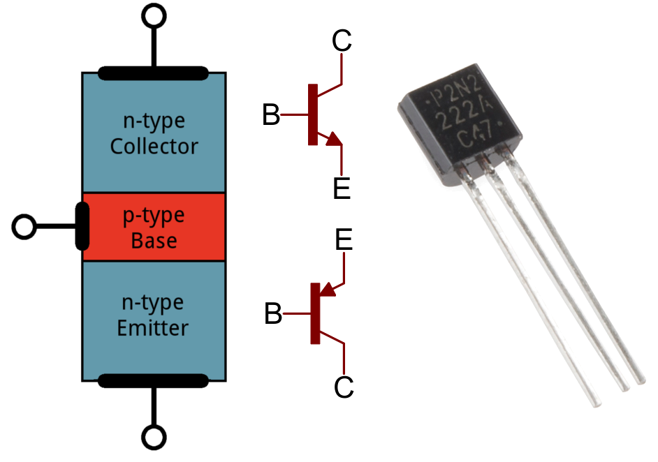
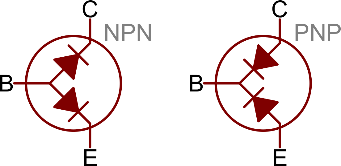
Transistors are fundamentally three-terminal devices. On a bi-polar junction transistor (BJT), those pins are labeled collector (C), base (B), and emitter (E). The circuit symbols for both the NPN and PNP BJT are below:
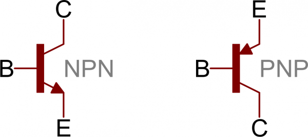 The only difference between an NPN and PNP is the direction of the arrow on the emitter. The arrow on an NPN points out, and on the PNP it points in. A useful mnemonic for remembering which is which is:
Transistors are fundamentally three-terminal devices. On a bi-polar junction transistor (BJT), those pins are labeled collector (C), base (B), and emitter (E). The circuit symbols for both the NPN and PNP BJT are below:
The only difference between an NPN and PNP is the direction of the arrow on the emitter. The arrow on an NPN points out, and on the PNP it points in. A useful mnemonic for remembering which is which is:
NPN: Not Pointing iN
Backwards logic, but it works!
Backwards logic, but it works!
Transistor Construction
Transistors rely on semiconductors to work their magic. A semiconductor is a material that’s not quite a pure conductor (like copper wire) but also not an insulator (like air). The conductivity of a semiconductor – how easily it allows electrons to flow – depends on variables like temperature or the presence of more or less electrons. Let’s look briefly under the hood of a transistor. Don’t worry, we won’t dig too deeply into quantum physics.
Transistors rely on semiconductors to work their magic. A semiconductor is a material that’s not quite a pure conductor (like copper wire) but also not an insulator (like air). The conductivity of a semiconductor – how easily it allows electrons to flow – depends on variables like temperature or the presence of more or less electrons. Let’s look briefly under the hood of a transistor. Don’t worry, we won’t dig too deeply into quantum physics.
A Transistor as Two Diodes
Transistors are kind of like an extension of another semiconductor component: diodes. In a way transistors are just two diodes with their cathodes (or anodes) tied together:
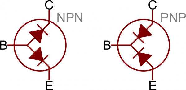 The diode connecting base to emitter is the important one here; it matches the direction of the arrow on the schematic symbol, and shows you which way current is intended to flow through the transistor.
The diode representation is a good place to start, but it’s far from accurate. Don’t base your understanding of a transistor’s operation on that model (and definitely don’t try to replicate it on a breadboard, it won’t work). There’s a whole lot of weird quantum physics level stuff controlling the interactions between the three terminals.
(This model is useful if you need to test a transistor. Using the diode (or resistance) test function on a multimeter, you can measure across the BE and BC terminals to check for the presence of those “diodes”.)
The diode connecting base to emitter is the important one here; it matches the direction of the arrow on the schematic symbol, and shows you which way current is intended to flow through the transistor.
The diode representation is a good place to start, but it’s far from accurate. Don’t base your understanding of a transistor’s operation on that model (and definitely don’t try to replicate it on a breadboard, it won’t work). There’s a whole lot of weird quantum physics level stuff controlling the interactions between the three terminals.
(This model is useful if you need to test a transistor. Using the diode (or resistance) test function on a multimeter, you can measure across the BE and BC terminals to check for the presence of those “diodes”.)
Transistors are kind of like an extension of another semiconductor component: diodes. In a way transistors are just two diodes with their cathodes (or anodes) tied together:
The diode connecting base to emitter is the important one here; it matches the direction of the arrow on the schematic symbol, and shows you which way current is intended to flow through the transistor.
The diode representation is a good place to start, but it’s far from accurate. Don’t base your understanding of a transistor’s operation on that model (and definitely don’t try to replicate it on a breadboard, it won’t work). There’s a whole lot of weird quantum physics level stuff controlling the interactions between the three terminals.
(This model is useful if you need to test a transistor. Using the diode (or resistance) test function on a multimeter, you can measure across the BE and BC terminals to check for the presence of those “diodes”.)
Transistor Structure and Operation
Transistors are built by stacking three different layers of semiconductor material together. Some of those layers have extra electrons added to them (a process called “doping”), and others have electrons removed (doped with “holes” – the absence of electrons). A semiconductor material with extra electrons is called an n-type (n for negative because electrons have a negative charge) and a material with electrons removed is called a p-type (for positive). Transistors are created by either stacking an n on top of a p on top of an n, or p over n over p.
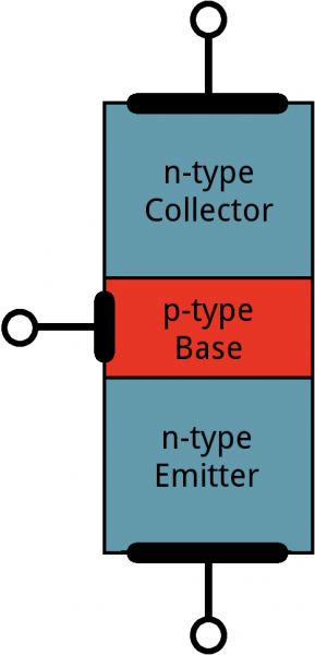 Simplified diagram of the structure of an NPN. Notice the origin of any acronyms?
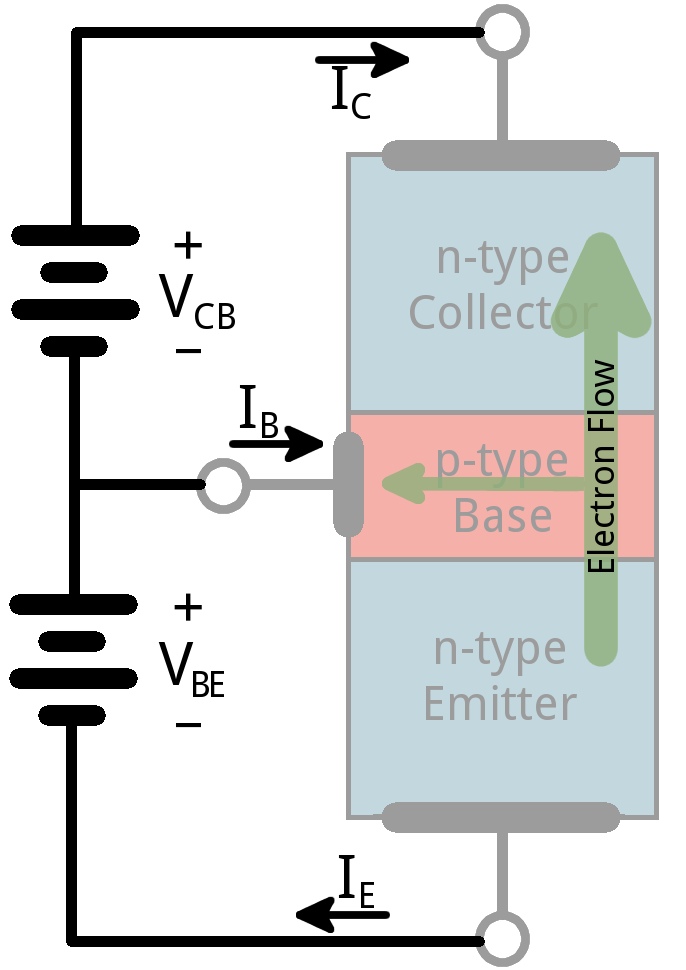
With some hand waving, we can say electrons can easily flow from n regions to p regions, as long as they have a little force (voltage) to push them. But flowing from a p region to an n region is really hard (requires a lot of voltage). But the special thing about a transistor – the part that makes our two-diode model obsolete – is the fact that electrons can easily flow from the p-type base to the n-type collector as long as the base-emitter junction is forward biased (meaning the base is at a higher voltage than the emitter).
Simplified diagram of the structure of an NPN. Notice the origin of any acronyms?
With some hand waving, we can say electrons can easily flow from n regions to p regions, as long as they have a little force (voltage) to push them. But flowing from a p region to an n region is really hard (requires a lot of voltage). But the special thing about a transistor – the part that makes our two-diode model obsolete – is the fact that electrons can easily flow from the p-type base to the n-type collector as long as the base-emitter junction is forward biased (meaning the base is at a higher voltage than the emitter).
 The NPN transistor is designed to pass electrons from the emitter to the collector (so conventional current flows from collector to emitter). The emitter “emits” electrons into the base, which controls the number of electrons the emitter emits. Most of the electrons emitted are “collected” by the collector, which sends them along to the next part of the circuit.
A PNP works in a same but opposite fashion. The base still controls current flow, but that current flows in the opposite direction – from emitter to collector. Instead of electrons, the emitter emits “holes” (a conceptual absence of electrons) which are collected by the collector.
The transistor is kind of like an electron valve. The base pin is like a handle you might adjust to allow more or less electrons to flow from emitter to collector. Let’s investigate this analogy further…
The NPN transistor is designed to pass electrons from the emitter to the collector (so conventional current flows from collector to emitter). The emitter “emits” electrons into the base, which controls the number of electrons the emitter emits. Most of the electrons emitted are “collected” by the collector, which sends them along to the next part of the circuit.
A PNP works in a same but opposite fashion. The base still controls current flow, but that current flows in the opposite direction – from emitter to collector. Instead of electrons, the emitter emits “holes” (a conceptual absence of electrons) which are collected by the collector.
The transistor is kind of like an electron valve. The base pin is like a handle you might adjust to allow more or less electrons to flow from emitter to collector. Let’s investigate this analogy further…
Transistors are built by stacking three different layers of semiconductor material together. Some of those layers have extra electrons added to them (a process called “doping”), and others have electrons removed (doped with “holes” – the absence of electrons). A semiconductor material with extra electrons is called an n-type (n for negative because electrons have a negative charge) and a material with electrons removed is called a p-type (for positive). Transistors are created by either stacking an n on top of a p on top of an n, or p over n over p.
Simplified diagram of the structure of an NPN. Notice the origin of any acronyms?
With some hand waving, we can say electrons can easily flow from n regions to p regions, as long as they have a little force (voltage) to push them. But flowing from a p region to an n region is really hard (requires a lot of voltage). But the special thing about a transistor – the part that makes our two-diode model obsolete – is the fact that electrons can easily flow from the p-type base to the n-type collector as long as the base-emitter junction is forward biased (meaning the base is at a higher voltage than the emitter).
The NPN transistor is designed to pass electrons from the emitter to the collector (so conventional current flows from collector to emitter). The emitter “emits” electrons into the base, which controls the number of electrons the emitter emits. Most of the electrons emitted are “collected” by the collector, which sends them along to the next part of the circuit.
A PNP works in a same but opposite fashion. The base still controls current flow, but that current flows in the opposite direction – from emitter to collector. Instead of electrons, the emitter emits “holes” (a conceptual absence of electrons) which are collected by the collector.
The transistor is kind of like an electron valve. The base pin is like a handle you might adjust to allow more or less electrons to flow from emitter to collector. Let’s investigate this analogy further…
Extending the Water Analogy
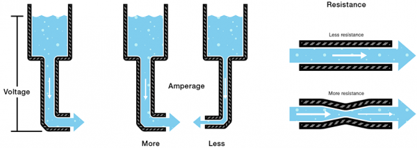
If you’ve been reading a lot of electricity concept tutorials lately, you’re probably used to water analogies. We say that current is analogous to the flow rate of water, voltage is the pressure pushing that water through a pipe, and resistance is the width of the pipe.
 Unsurprisingly, the water analogy can be extended to transistors as well: a transistor is like a water valve – a mechanism we can use to control the flow rate.
There are three states we can use a valve in, each of which has a different effect on the flow rate in a system.
Unsurprisingly, the water analogy can be extended to transistors as well: a transistor is like a water valve – a mechanism we can use to control the flow rate.
There are three states we can use a valve in, each of which has a different effect on the flow rate in a system.
If you’ve been reading a lot of electricity concept tutorials lately, you’re probably used to water analogies. We say that current is analogous to the flow rate of water, voltage is the pressure pushing that water through a pipe, and resistance is the width of the pipe.

Unsurprisingly, the water analogy can be extended to transistors as well: a transistor is like a water valve – a mechanism we can use to control the flow rate.
There are three states we can use a valve in, each of which has a different effect on the flow rate in a system.
1) On – Short Circuit
A valve can be completely opened, allowing water to flow freely – passing through as if the valve wasn’t even present.
 Likewise, under the right circumstances, a transistor can look like a short circuit between the collector and emitter pins. Current is free to flow through the collector, and out the emitter.
A valve can be completely opened, allowing water to flow freely – passing through as if the valve wasn’t even present.
Likewise, under the right circumstances, a transistor can look like a short circuit between the collector and emitter pins. Current is free to flow through the collector, and out the emitter.
2) Off – Open Circuit
When it’s closed, a valve can completely stop the flow of water.
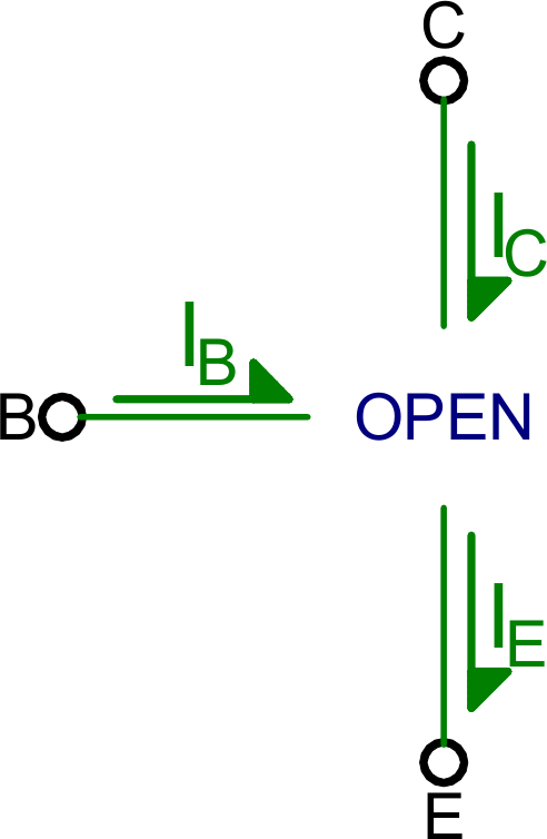
 In the same way, a transistor can be used to create an open circuit between the collector and emitter pins.
When it’s closed, a valve can completely stop the flow of water.
In the same way, a transistor can be used to create an open circuit between the collector and emitter pins.
3) Linear Flow Control
With some precise tuning, a valve can be adjusted to finely control the flow rate to some point between fully open and closed.
 A transistor can do the same thing – linearly controlling the current through a circuit at some point between fully off (an open circuit) and fully on (a short circuit).
From our water analogy, the width of a pipe is similar to the resistance in a circuit. If a valve can finely adjust the width of a pipe, then a transistor can finely adjust the resistance between collector and emitter. So, in a way, a transistor is like a variable, adjustable resistor.
A transistor can do the same thing – linearly controlling the current through a circuit at some point between fully off (an open circuit) and fully on (a short circuit).
From our water analogy, the width of a pipe is similar to the resistance in a circuit. If a valve can finely adjust the width of a pipe, then a transistor can finely adjust the resistance between collector and emitter. So, in a way, a transistor is like a variable, adjustable resistor.
With some precise tuning, a valve can be adjusted to finely control the flow rate to some point between fully open and closed.
A transistor can do the same thing – linearly controlling the current through a circuit at some point between fully off (an open circuit) and fully on (a short circuit).
From our water analogy, the width of a pipe is similar to the resistance in a circuit. If a valve can finely adjust the width of a pipe, then a transistor can finely adjust the resistance between collector and emitter. So, in a way, a transistor is like a variable, adjustable resistor.
Amplifying Power
There’s another analogy we can wrench into this. Imagine if, with the slight turn of a valve, you could control the flow rate of the Hoover Dam’s flow gates. The measly amount of force you might put into twisting that knob has the potential to create a force thousands of times stronger. We’re stretching the analogy to its limits, but this idea carries over to transistors too. Transistors are special because they can amplify electrical signals, turning a low-power signal into a similar signal of much higher power.
Kind of. There’s a lot more to it, but that’s a good place to start! Check out the next section for a more detailed explanation of the operation of a transistor.
Operation Modes
Unlike resistors, which enforce a linear relationship between voltage and current, transistors are non-linear devices. They have four distinct modes of operation, which describe the current flowing through them. (When we talk about current flow through a transistor, we usually mean current flowing from collector to emitter of an NPN.)
The four transistor operation modes are:
- Saturation – The transistor acts like a short circuit. Current freely flows from collector to emitter.
- Cut-off – The transistor acts like an open circuit. No current flows from collector to emitter.
- Active – The current from collector to emitter is proportional to the current flowing into the base.
- Reverse-Active – Like active mode, the current is proportional to the base current, but it flows in reverse. Current flows from emitter to collector (not, exactly, the purpose transistors were designed for).
To determine which mode a transistor is in, we need to look at the voltages on each of the three pins, and how they relate to each other. The voltages from base to emitter (VBE), and the from base to collector (VBC) set the transistor’s mode:
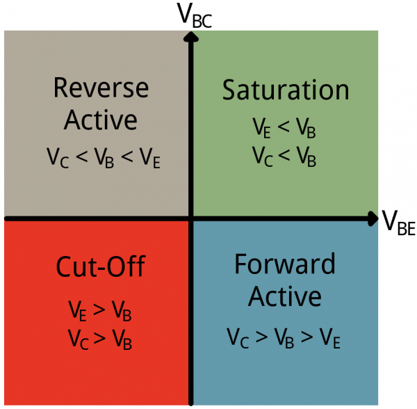 The simplified quadrant graph above shows how positive and negative voltages at those terminals affect the mode. In reality it’s a bit more complicated than that.
Let’s look at all four transistor modes individually; we’ll investigate how to put the device into that mode, and what effect it has on current flow.
Note: The majority of this page focuses on NPN transistors. To understand how a PNP transistor works, simply flip the polarity or > and < signs.
The simplified quadrant graph above shows how positive and negative voltages at those terminals affect the mode. In reality it’s a bit more complicated than that.
Let’s look at all four transistor modes individually; we’ll investigate how to put the device into that mode, and what effect it has on current flow.
Note: The majority of this page focuses on NPN transistors. To understand how a PNP transistor works, simply flip the polarity or > and < signs.
Unlike resistors, which enforce a linear relationship between voltage and current, transistors are non-linear devices. They have four distinct modes of operation, which describe the current flowing through them. (When we talk about current flow through a transistor, we usually mean current flowing from collector to emitter of an NPN.)
The four transistor operation modes are:
- Saturation – The transistor acts like a short circuit. Current freely flows from collector to emitter.
- Cut-off – The transistor acts like an open circuit. No current flows from collector to emitter.
- Active – The current from collector to emitter is proportional to the current flowing into the base.
- Reverse-Active – Like active mode, the current is proportional to the base current, but it flows in reverse. Current flows from emitter to collector (not, exactly, the purpose transistors were designed for).
To determine which mode a transistor is in, we need to look at the voltages on each of the three pins, and how they relate to each other. The voltages from base to emitter (VBE), and the from base to collector (VBC) set the transistor’s mode:
The simplified quadrant graph above shows how positive and negative voltages at those terminals affect the mode. In reality it’s a bit more complicated than that.
Let’s look at all four transistor modes individually; we’ll investigate how to put the device into that mode, and what effect it has on current flow.
Note: The majority of this page focuses on NPN transistors. To understand how a PNP transistor works, simply flip the polarity or > and < signs.
Saturation Mode
Saturation is the on mode of a transistor. A transistor in saturation mode acts like a short circuit between collector and emitter.
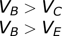
 In saturation mode both of the “diodes” in the transistor are forward biased. That means VBE must be greater than 0, and so must VBC. In other words, VB must be higher than both VE and VC.
 Because the junction from base to emitter looks just like a diode, in reality, VBE must be greater than a threshold voltage to enter saturation. There are many abbreviations for this voltage drop – Vth, Vγ, and Vd are a few – and the actual value varies between transistors (and even further by temperature). For a lot of transistors (at room temperature) we can estimate this drop to be about 0.6V.
Another reality bummer: there won’t be perfect conduction between emitter and collector. A small voltage drop will form between those nodes. Transistor datasheets will define this voltage as CE saturation voltage VCE(sat) – a voltage from collector to emitter required for saturation. This value is usually around 0.05-0.2V. This value means that VC must be slightly greater than VE (but both still less than VB) to get the transistor in saturation mode.
Because the junction from base to emitter looks just like a diode, in reality, VBE must be greater than a threshold voltage to enter saturation. There are many abbreviations for this voltage drop – Vth, Vγ, and Vd are a few – and the actual value varies between transistors (and even further by temperature). For a lot of transistors (at room temperature) we can estimate this drop to be about 0.6V.
Another reality bummer: there won’t be perfect conduction between emitter and collector. A small voltage drop will form between those nodes. Transistor datasheets will define this voltage as CE saturation voltage VCE(sat) – a voltage from collector to emitter required for saturation. This value is usually around 0.05-0.2V. This value means that VC must be slightly greater than VE (but both still less than VB) to get the transistor in saturation mode.
Saturation is the on mode of a transistor. A transistor in saturation mode acts like a short circuit between collector and emitter.

In saturation mode both of the “diodes” in the transistor are forward biased. That means VBE must be greater than 0, and so must VBC. In other words, VB must be higher than both VE and VC.
Because the junction from base to emitter looks just like a diode, in reality, VBE must be greater than a threshold voltage to enter saturation. There are many abbreviations for this voltage drop – Vth, Vγ, and Vd are a few – and the actual value varies between transistors (and even further by temperature). For a lot of transistors (at room temperature) we can estimate this drop to be about 0.6V.
Another reality bummer: there won’t be perfect conduction between emitter and collector. A small voltage drop will form between those nodes. Transistor datasheets will define this voltage as CE saturation voltage VCE(sat) – a voltage from collector to emitter required for saturation. This value is usually around 0.05-0.2V. This value means that VC must be slightly greater than VE (but both still less than VB) to get the transistor in saturation mode.
Cutoff Mode
Cutoff mode is the opposite of saturation. A transistor in cutoff mode is off – there is no collector current, and therefore no emitter current. It almost looks like an open circuit.
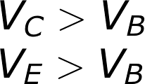
 To get a transistor into cutoff mode, the base voltage must be less than both the emitter and collector voltages. VBCand VBE must both be negative.
 In reality, VBE can be anywhere between 0V and Vth (~0.6V) to achieve cutoff mode.
Cutoff mode is the opposite of saturation. A transistor in cutoff mode is off – there is no collector current, and therefore no emitter current. It almost looks like an open circuit.
To get a transistor into cutoff mode, the base voltage must be less than both the emitter and collector voltages. VBCand VBE must both be negative.
In reality, VBE can be anywhere between 0V and Vth (~0.6V) to achieve cutoff mode.
Active Mode
To operate in active mode, a transistor’s VBE must be greater than zero and VBC must be negative. Thus, the base voltage must be less than the collector, but greater than the emitter. That also means the collector must be greater than the emitter.
 In reality, we need a non-zero forward voltage drop (abbreviated either Vth, Vγ, or Vd) from base to emitter (VBE) to “turn on” the transistor. Usually this voltage is usually around 0.6V.
To operate in active mode, a transistor’s VBE must be greater than zero and VBC must be negative. Thus, the base voltage must be less than the collector, but greater than the emitter. That also means the collector must be greater than the emitter.
In reality, we need a non-zero forward voltage drop (abbreviated either Vth, Vγ, or Vd) from base to emitter (VBE) to “turn on” the transistor. Usually this voltage is usually around 0.6V.
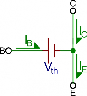
Amplifying in Active Mode
Active mode is the most powerful mode of the transistor because it turns the device into an amplifier. Current going into the base pin amplifies current going into the collector and out the emitter.
Our shorthand notation for the gain (amplification factor) of a transistor is β (you may also see it as βF, or hFE). β linearly relates the collector current (IC) to the base current (IB):
 The actual value of β varies by transistor. It’s usually around 100, but can range from 50 to 200…even 2000, depending on which transistor you’re using and how much current is running through it. If your transistor had a β of 100, for example, that’d mean an input current of 1mA into the base could produce 100mA current through the collector.
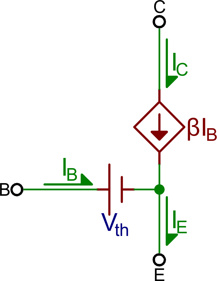
 Active mode model. VBE = Vth, and IC = βIB.
What about the emitter current, IE? In active mode, the collector and base currents go into the device, and the IEcomes out. To relate the emitter current to collector current, we have another constant value: α. α is the common-base current gain, it relates those currents as such:
Active mode model. VBE = Vth, and IC = βIB.
What about the emitter current, IE? In active mode, the collector and base currents go into the device, and the IEcomes out. To relate the emitter current to collector current, we have another constant value: α. α is the common-base current gain, it relates those currents as such:
 α is usually very close to, but less than, 1. That means IC is very close to, but less than IE in active mode.
You can use β to calculate α, or vice-versa:
α is usually very close to, but less than, 1. That means IC is very close to, but less than IE in active mode.
You can use β to calculate α, or vice-versa:
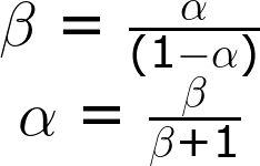 If β is 100, for example, that means α is 0.99. So, if IC is 100mA, for example, then IE is 101mA.
Active mode is the most powerful mode of the transistor because it turns the device into an amplifier. Current going into the base pin amplifies current going into the collector and out the emitter.
Our shorthand notation for the gain (amplification factor) of a transistor is β (you may also see it as βF, or hFE). β linearly relates the collector current (IC) to the base current (IB):
The actual value of β varies by transistor. It’s usually around 100, but can range from 50 to 200…even 2000, depending on which transistor you’re using and how much current is running through it. If your transistor had a β of 100, for example, that’d mean an input current of 1mA into the base could produce 100mA current through the collector.
Active mode model. VBE = Vth, and IC = βIB.
What about the emitter current, IE? In active mode, the collector and base currents go into the device, and the IEcomes out. To relate the emitter current to collector current, we have another constant value: α. α is the common-base current gain, it relates those currents as such:
α is usually very close to, but less than, 1. That means IC is very close to, but less than IE in active mode.
You can use β to calculate α, or vice-versa:
If β is 100, for example, that means α is 0.99. So, if IC is 100mA, for example, then IE is 101mA.
Reverse Active
Just as saturation is the opposite of cutoff, reverse active mode is the opposite of active mode. A transistor in reverse active mode conducts, even amplifies, but current flows in the opposite direction, from emitter to collector. The downside to reverse active mode is the β (βR in this case) is much smaller.
To put a transistor in reverse active mode, the emitter voltage must be greater than the base, which must be greater than the collector (VBE<0 and VBC>0).
 Reverse active mode isn’t usually a state in which you want to drive a transistor. It’s good to know it’s there, but it’s rarely designed into an application.
Just as saturation is the opposite of cutoff, reverse active mode is the opposite of active mode. A transistor in reverse active mode conducts, even amplifies, but current flows in the opposite direction, from emitter to collector. The downside to reverse active mode is the β (βR in this case) is much smaller.
To put a transistor in reverse active mode, the emitter voltage must be greater than the base, which must be greater than the collector (VBE<0 and VBC>0).
Reverse active mode isn’t usually a state in which you want to drive a transistor. It’s good to know it’s there, but it’s rarely designed into an application.

Comments
Post a Comment